Solar Panels Made With a Particle Accelerator?!
Based on minutephysics's video on YouTube. If you like this content, support the original creators by watching, liking and subscribing to their content.
Conventional saw cutting wastes silicon because the kerf gap can be about as wide as the wafer, and very thin wafers are prone to breakage.
Briefing
Particle accelerators can help make solar panels by solving a mundane but costly bottleneck in silicon wafer production: how to cut extremely thin silicon slices without wasting half the material. Traditional saw-based cutting struggles at wafer thicknesses around 0.15 millimeters because the blade both risks breaking the wafer and creates a wide “kerf” gap—material ground away by the teeth. For silicon, that kerf can be roughly as wide as the wafer itself, meaning about half of the original silicon ends up as waste.
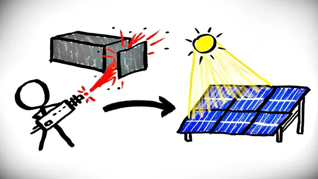
The alternative uses crystal physics rather than brute-force cutting. A silicon solar cell starts as a carefully grown cylindrical crystal of silicon atoms arranged in a regular lattice. Instead of slicing the cylinder with a saw, manufacturers can bombard the flat face with protons at a chosen energy. Those protons embed into the silicon, with penetration depth controlled by the proton energy—so the target wafer thickness can be set by how much energy the protons carry. Once inside, the protons disrupt the crystal lattice and generate internal stress along the implanted region.
After the proton implantation step, the process turns that built-in stress into a clean separation. Heating the silicon causes the stressed region to cleave along the crystal lattice lines where the protons were embedded. The result is a wafer that breaks off cleanly rather than being physically gouged away. To make the cleaved wafer usable, it can be glued onto a supporting substrate—glass or plastic—before heating. That way, the thin silicon wafer ends up attached to a durable (and potentially flexible) backing, with essentially no silicon lost to cutting debris.
The economic logic hinges on material efficiency. A particle accelerator is far more expensive than a saw, but the method uses significantly less silicon per wafer and avoids kerf waste. That opens the door to using higher-cost silicon that performs better at capturing sunlight. If more efficient silicon allows smaller, lower-bulk panels for the same power output—and reduces the amount of other materials needed to support and package the cells—then the savings could offset the accelerator’s added cost.
Commercialization is still a steep climb. Rayton Solar is pursuing this proton-implantation approach for large-scale solar cell manufacturing and is seeking investors. The effort is framed as a challenging, capital-intensive path, but the underlying idea is straightforward: replace wasteful mechanical cutting with a controlled, lattice-based cleaving mechanism that turns expensive silicon into more usable product per kilogram.
Cornell Notes
Solar panels rely on thin silicon wafers, but conventional saw cutting wastes a large fraction of the silicon because the kerf gap is wide and the wafer can break at thicknesses near 0.15 millimeters. A particle-accelerator method avoids kerf loss by implanting protons into a silicon crystal: proton energy sets how deep they penetrate, and the implanted region creates stress that cleaves cleanly along crystal lattice lines when heated. By gluing the “proto-wafer” to a glass or plastic substrate before heating, manufacturers can obtain a thin wafer attached to a durable backing with essentially no cutting debris. The main tradeoff is cost: accelerators are expensive, but improved silicon utilization could justify using more efficient, higher-cost silicon and reduce overall panel size and supporting materials.
Why does saw cutting waste so much silicon when making solar wafers?
How does proton implantation control the thickness of the silicon wafer?
What physical mechanism makes the silicon cleave cleanly after implantation?
Why glue the proto-wafer to glass or plastic before heating?
What economic tradeoff determines whether the accelerator method could win?
Who is attempting to commercialize this approach?
Review Questions
- How does proton energy determine the cleaving plane and final wafer thickness in the accelerator-based method?
- What specific role does kerf waste play in the cost structure of conventional silicon wafer production?
- What conditions (implantation, gluing, heating) must occur in sequence to produce a usable thin wafer without debris?
Key Points
- 1
Conventional saw cutting wastes silicon because the kerf gap can be about as wide as the wafer, and very thin wafers are prone to breakage.
- 2
Proton implantation embeds into silicon, with implantation depth set by proton energy, enabling precise control of wafer thickness.
- 3
Implanted protons create stress in the silicon crystal lattice, and heating triggers clean cleaving along lattice lines.
- 4
Gluing the proto-wafer to glass or plastic before heating allows the cleaved thin silicon wafer to remain attached to a durable backing.
- 5
The main advantage is near-zero cutting waste, which could make higher-cost, higher-efficiency silicon economically viable.
- 6
The key downside is that particle accelerators are expensive, so commercialization depends on whether material savings and panel downsizing offset accelerator costs.
- 7
Rayton Solar is working toward commercial-scale implementation and is seeking investors to fund the effort.