The World's Most Important Machine
Based on Veritasium's video on YouTube. If you like this content, support the original creators by watching, liking and subscribing to their content.
Moore’s Law stalled when photolithography hit diffraction and numerical-aperture limits, making 193 nm deep UV tools insufficient for further scaling.
Briefing
Moore’s Law didn’t stall because chipmakers ran out of ideas—it stalled because photolithography hit physical limits, and the industry needed an “impossible” machine to keep shrinking transistors. Extreme ultraviolet lithography (EUV) became that lifeline: a system that can print features at nanometer scales by generating 13.4 nm EUV light, reflecting it off ultra-smooth multilayer mirrors, and aligning multiple chip layers with about one nanometer of overlay error—roughly five silicon atoms.
The bottleneck traces back to how chip patterns get transferred. Traditional photolithography shines light through a mask, but as feature sizes approach the light’s wavelength, diffraction and interference distort the image. Designers can fight this with larger numerical aperture optics, but numerical aperture has a ceiling. The industry therefore kept moving to shorter wavelengths—eventually settling on 193 nm deep UV—until around 2015 when further shrinking became untenable. EUV offered a new route: use much shorter wavelengths (around 13 nm) so diffraction blurs less, but that introduces a cascade of engineering problems.
Early x-ray lithography work hinted at the path but faced skepticism and practical barriers. Hiroo Kinoshita proposed using ~10 nm x-rays, yet x-rays are absorbed by air and require vacuum systems and mirrors smooth on atomic scales. Curved multilayer mirrors—built from alternating tungsten and carbon layers—proved x-rays could be reflected, but the reflectivity and infrastructure demands made the approach feel unrealistic. Similar efforts at Lawrence Livermore National Laboratory and later Bell Labs partnerships helped keep x-ray lithography alive long enough for the field to pivot toward EUV.
EUV’s core challenge is efficiency. EUV light at 13.4 nm must bounce off multiple mirrors (including a reflective reticle), and each reflection loses power. Even with ~70% reflectivity per mirror, repeated bounces drain photons quickly, forcing the system to generate far more EUV power than early prototypes could deliver. The solution required a scalable EUV light source and a way to protect the collector mirror from debris.
ASML’s approach uses laser-produced plasma. A high-power laser hits a stream of tin droplets, heating them to extreme temperatures and producing EUV photons. Tin’s emission spectrum around 13.5 nm improves conversion efficiency compared with xenon, but the droplets also create debris that can foul the collector. The machine therefore runs with low-pressure hydrogen to slow and cool tin particles; any tin that reaches the collector is converted into stannane gas and removed while the system operates. Heat management became its own science problem—shockwaves in the hydrogen were modeled with the Taylor–von Neumann–Sedov framework, guiding the required hydrogen flushing speeds.
Power targets kept moving. Early EUV prototypes could print only about 10 wafers per hour, while manufacturing viability demanded hundreds of wafers per hour. ASML and its partners (notably Zeiss for optics) pushed source power from tens of watts toward 100 watts and beyond, using multi-pulse laser schemes that first “pancake” the droplet and then ionize it more effectively. They also had to solve timing: droplets travel through a turbulent hydrogen flow, so laser pulses must hit each droplet with golf-ball precision through a tornado.
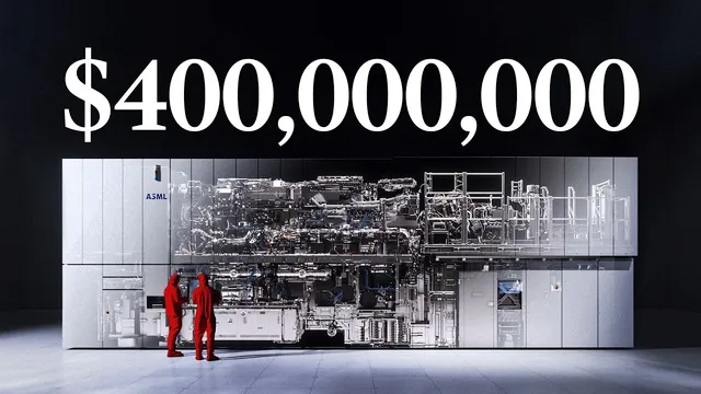
By 2016, orders began flowing, and the latest systems expanded optical performance with higher numerical aperture (0.55) to print smaller features. The result is a machine so complex it’s shipped in thousands of parts and tens of trucks—yet it’s now embedded in the supply chain behind today’s most advanced chips. The central takeaway is that EUV succeeded only after decades of iterative breakthroughs across optics, plasma physics, contamination control, and precision metrology—turning a “brick wall” into a manufacturing reality.
Cornell Notes
Moore’s Law stalled when photolithography reached a diffraction limit: as mask gaps shrink toward the wavelength, interference and blur prevent further feature scaling. EUV (extreme ultraviolet lithography) sidestepped this by using ~13.4 nm light, but it demanded a new kind of lithography machine with extremely efficient optics and precise layer alignment. ASML’s solution uses laser-produced plasma from tin droplets to generate EUV, then relies on multilayer mirrors and a reflective reticle to project the pattern onto wafers. The system also had to protect atomically smooth collector mirrors from debris using low-pressure hydrogen and carefully tuned gas flow. After decades of setbacks, EUV became commercially viable and now underpins advanced chip manufacturing.
Why did shrinking transistor features stop working with 193 nm deep UV lithography?
What makes EUV fundamentally different from earlier lithography approaches?
How does ASML generate EUV light, and why tin beat xenon?
How does the machine prevent tin debris from ruining the collector mirror?
Why is overlay accuracy around one nanometer such a big deal for EUV manufacturing?
What engineering breakthrough helped raise EUV source power toward viable wafer throughput?
Review Questions
- What physical limit in optical projection makes feature scaling harder as mask gaps approach the wavelength?
- Why does reflective multilayer optics force EUV systems to chase much higher source power than earlier lithography?
- How do hydrogen gas dynamics and mirror contamination control interact in keeping EUV tools productive?
Key Points
- 1
Moore’s Law stalled when photolithography hit diffraction and numerical-aperture limits, making 193 nm deep UV tools insufficient for further scaling.
- 2
EUV works at ~13.4 nm but requires reflective multilayer optics, where each mirror bounce reduces photon throughput and forces much higher source power.
- 3
ASML’s EUV light source uses laser-produced plasma from tin droplets; tin improves conversion efficiency compared with xenon by better matching the emission spectrum to mirror reflectivity.
- 4
Low-pressure hydrogen both protects the collector mirror from tin debris and must be tuned to avoid EUV absorption and overheating.
- 5
EUV manufacturing depends on extreme overlay control—about one nanometer—because misalignment of only a few atoms can break device performance.
- 6
Multi-pulse laser schemes that flatten droplets into “pancakes” before ionization increased EUV yield and helped push power toward manufacturing targets.
- 7
Timing and droplet synchronization are as critical as power: droplets travel through turbulent hydrogen flow, so laser pulses must hit each droplet with near-golf-ball precision.