Why It Was Almost Impossible to Make the Blue LED
Based on Veritasium's video on YouTube. If you like this content, support the original creators by watching, liking and subscribing to their content.
Blue LEDs required both near-perfect crystal quality and a workable p-type gallium nitride process; failures in either area stalled the industry for years.
Briefing
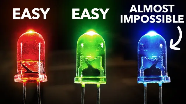
Blue LEDs were considered nearly impossible for decades because producing them required a near-perfect crystal and a reliable way to make p-type gallium nitride—two bottlenecks that stymied major electronics companies worldwide. The breakthrough came from Shūji Nakamura at Nichia, who ultimately delivered a true blue LED at 450 nanometers with enough brightness to be seen in daylight, then used that platform to enable white LEDs and transform modern lighting.
For years after Nick Holonyak’s first visible LED in 1962 (faint red) and Monsanto’s later green LED, LEDs were stuck at red and green. Blue was the missing ingredient: with red, green, and blue, manufacturers could mix colors to create white and essentially any other hue—unlocking LEDs for everything from bulbs and phones to TVs and billboards. Instead, the industry’s pursuit of blue repeatedly failed. Even as companies like IBM, GE, Bell Labs, and others poured resources into the problem, progress stalled for roughly a decade, and LED lighting remained mostly limited to indicators and small devices.
Nakamura’s path began at Nichia, where semiconductor efforts were struggling and internal pressure mounted. After supervisors effectively told him to quit, he gambled on a moonshot aimed at the elusive blue LED that others had missed. The key technical requirement was crystal quality: defects in the lattice disrupt electron flow, turning potential light emission into heat. Nakamura pursued Metal Organic Chemical Vapor Deposition (MOCVD), a method capable of mass-producing clean crystals, and spent time mastering it in Florida under a colleague’s lab setup.
Back in Japan, Nakamura focused on gallium nitride rather than the more popular zinc selenide route. Zinc selenide had a small lattice mismatch but lacked a known p-type method; gallium nitride was harder to grow and had enormous defect rates on sapphire, plus p-type had remained elusive. Nakamura’s first major leap was engineering the growth process itself. He built a “two-flow reactor” design that pinned reactant flow to the substrate to produce smoother, higher-mobility gallium nitride—so clean it could even serve as a buffer layer, improving subsequent layers.
The second hurdle was p-type gallium nitride. Earlier work by Isamu Akasaki and Hiroshi Amano showed magnesium-doped gallium nitride could become p-type only after electron-beam irradiation, but that approach was too slow for production. Nakamura found a scalable alternative: annealing magnesium-doped gallium nitride at about 400°C. The chemistry behind the fix was hydrogen—hydrogen from ammonia was bonding with magnesium and blocking holes, and added energy freed the holes again.
The final obstacle was boosting output power to practical levels. Nakamura used a carefully engineered active region based on indium gallium nitride to tune the band gap toward true blue, then corrected electron “overflow” by redesigning the well structure into a hill and adding aluminum gallium nitride to block leakage. By 1994, the result was a bright blue LED emitting at 450 nanometers with 1,500 microwatts—over 100 times brighter than earlier “pseudo-blue” devices. Nichia’s rapid scale-up followed, and by 1996 white LEDs emerged by coating the blue with yellow phosphor.
The payoff was enormous: Nichia’s revenue surged, and blue LEDs became foundational to the LED lighting revolution. Nakamura later faced legal battles over compensation and left Nichia in 2000, but his work—recognized by the Nobel Prize in physics in 2014—ultimately helped drive a shift in global residential lighting from 1% LED sales in 2010 to over half by 2022, with major carbon-emissions reductions expected as adoption accelerates.
Cornell Notes
Blue LEDs were blocked for decades by two linked problems: making near-perfect semiconductor crystals and achieving reliable p-type gallium nitride. Shūji Nakamura at Nichia overcame both by mastering MOCVD crystal growth and inventing a “two-flow reactor” that produced unusually smooth gallium nitride. He then solved the p-type bottleneck by showing that annealing magnesium-doped gallium nitride (around 400°C) releases holes that hydrogen had trapped, avoiding slow electron-beam irradiation. With an indium gallium nitride active layer tuned to the right band gap—and additional structures to prevent electron leakage—his team reached true blue emission at 450 nm and enough brightness for daylight. That breakthrough enabled white LEDs using yellow phosphor and reshaped global lighting.
Why did blue LEDs take so much longer than red and green?
What role did MOCVD play in Nakamura’s approach?
How did the “two-flow reactor” improve gallium nitride quality?
Why was p-type gallium nitride so hard, and what fixed it?
How did Nakamura reach true blue brightness instead of dim “pseudo-blue”?
What turned blue LEDs into white LEDs?
Review Questions
- What two material-science bottlenecks had to be solved to make a practical blue LED, and how did Nakamura address each one?
- Explain how hydrogen in ammonia interfered with p-type gallium nitride and why annealing worked when electron-beam irradiation was too slow.
- Describe the purpose of the indium gallium nitride active layer and the structural changes Nakamura made to prevent electron leakage.
Key Points
- 1
Blue LEDs required both near-perfect crystal quality and a workable p-type gallium nitride process; failures in either area stalled the industry for years.
- 2
MOCVD was central because it enabled controlled, thin-layer crystal growth on a lattice-matched substrate, but Nakamura had to modify the reactor to get gallium nitride to grow cleanly.
- 3
The “two-flow reactor” improved gallium nitride uniformity by pinning the reactant flow to the substrate while keeping the combined streams laminar.
- 4
Annealing magnesium-doped gallium nitride at about 400°C produced fully p-type material by freeing holes trapped by hydrogen from ammonia.
- 5
Nakamura’s output-power breakthrough relied on tuning the band gap with indium gallium nitride and redesigning the active-region structure to stop electron overflow.
- 6
Nichia’s white LED breakthrough came from converting blue light using yellow phosphor, enabling broad adoption of LED lighting.
- 7
Nakamura’s technical success did not translate into smooth corporate relations; later legal disputes centered on compensation for his invention.